Written by Stefan Nikolaj
19 Jul 2022
Obtaining a strange PLC
A few months ago, while talking with an amazing friend, I mentioned that I have an affinity towards old 8-bit microprocessors. The conversation then continued something like this: “Oh we were just about to throw away an old PLC with a Z80 on it.” “Why would you throw something like that away?” “The monitor interface is broken and the power supply is dead. The rest is fine. Do you want it?” “Is that a question?”
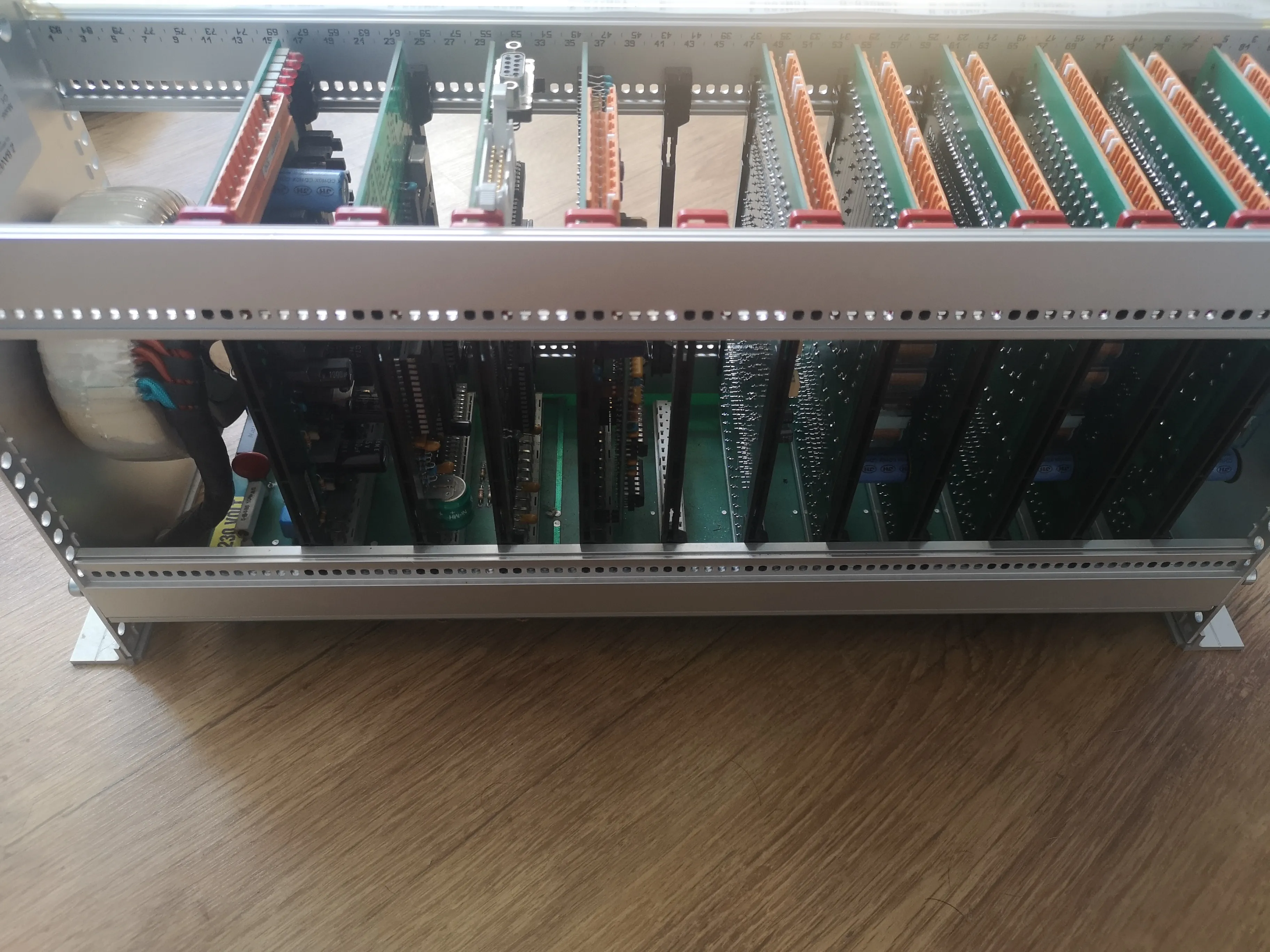
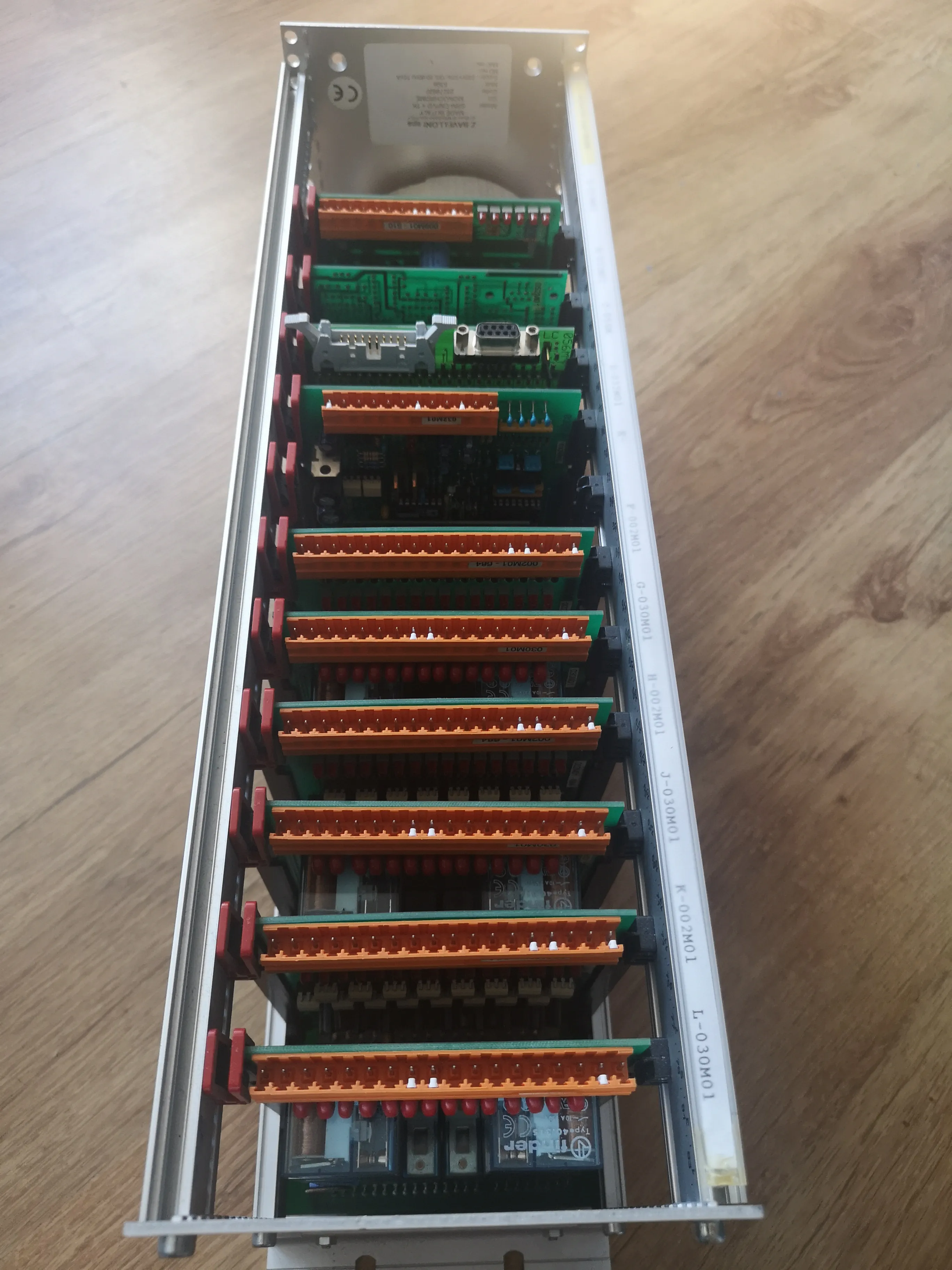
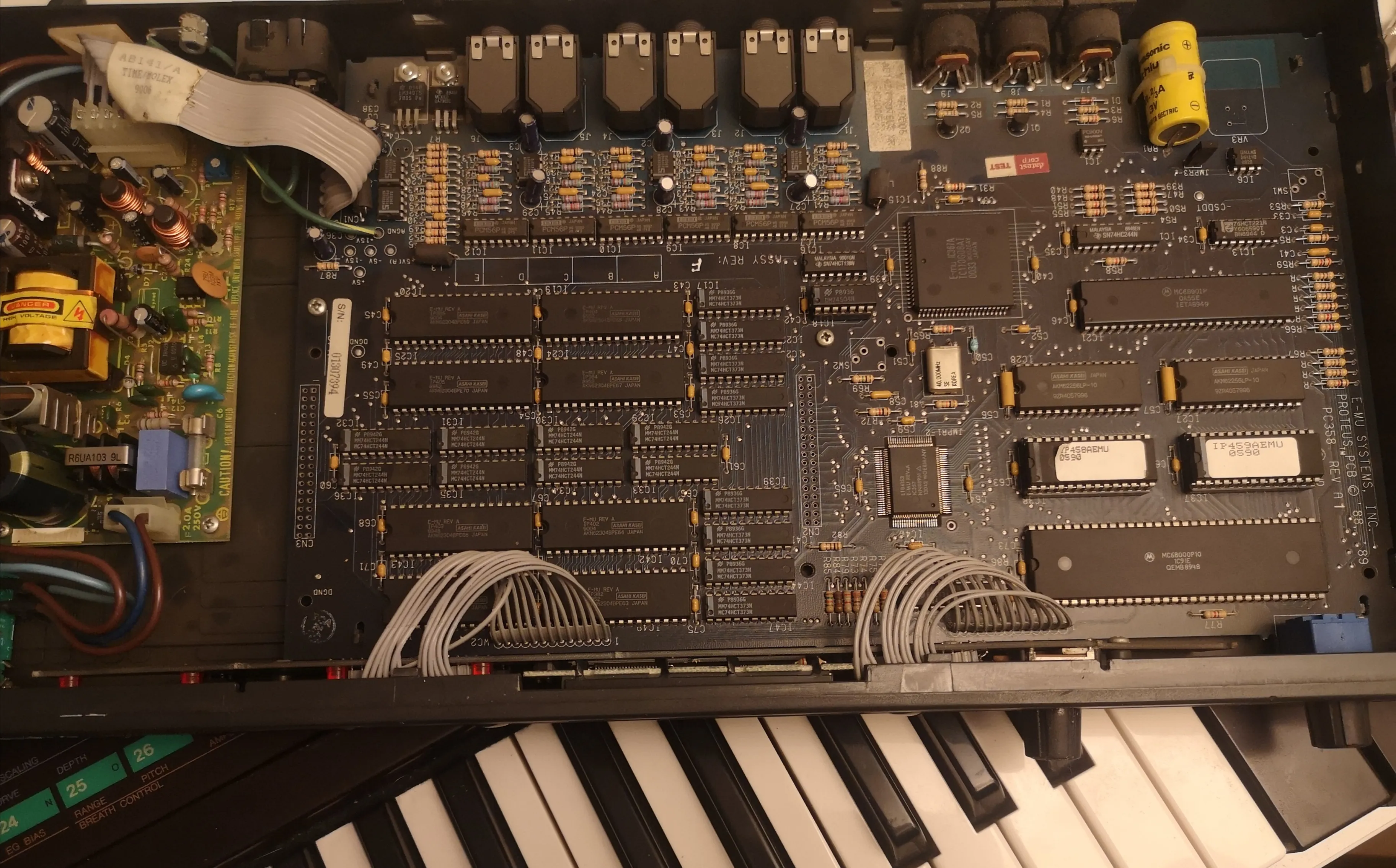
So, my friend sent the old PLC to me through the post, and after a short time it arrived with some other goodies. Initially, I admired the great construction, how it was made from interconnected boards with many DIP chips, beautifully routed together. Though the date codes on the chips indicated that they were from ~2004, the design looked like it was something straight out of the 80s. In this post, all the boards will be discussed and high-resolution pictures of them will be uploaded. Most of the parts and their markings should be visible, however if anyone cannot read a specific marking or wants to know more about a board, contact me and I can take higher resolution pictures of all sides and parts.
Exploring the boards - the graphics board
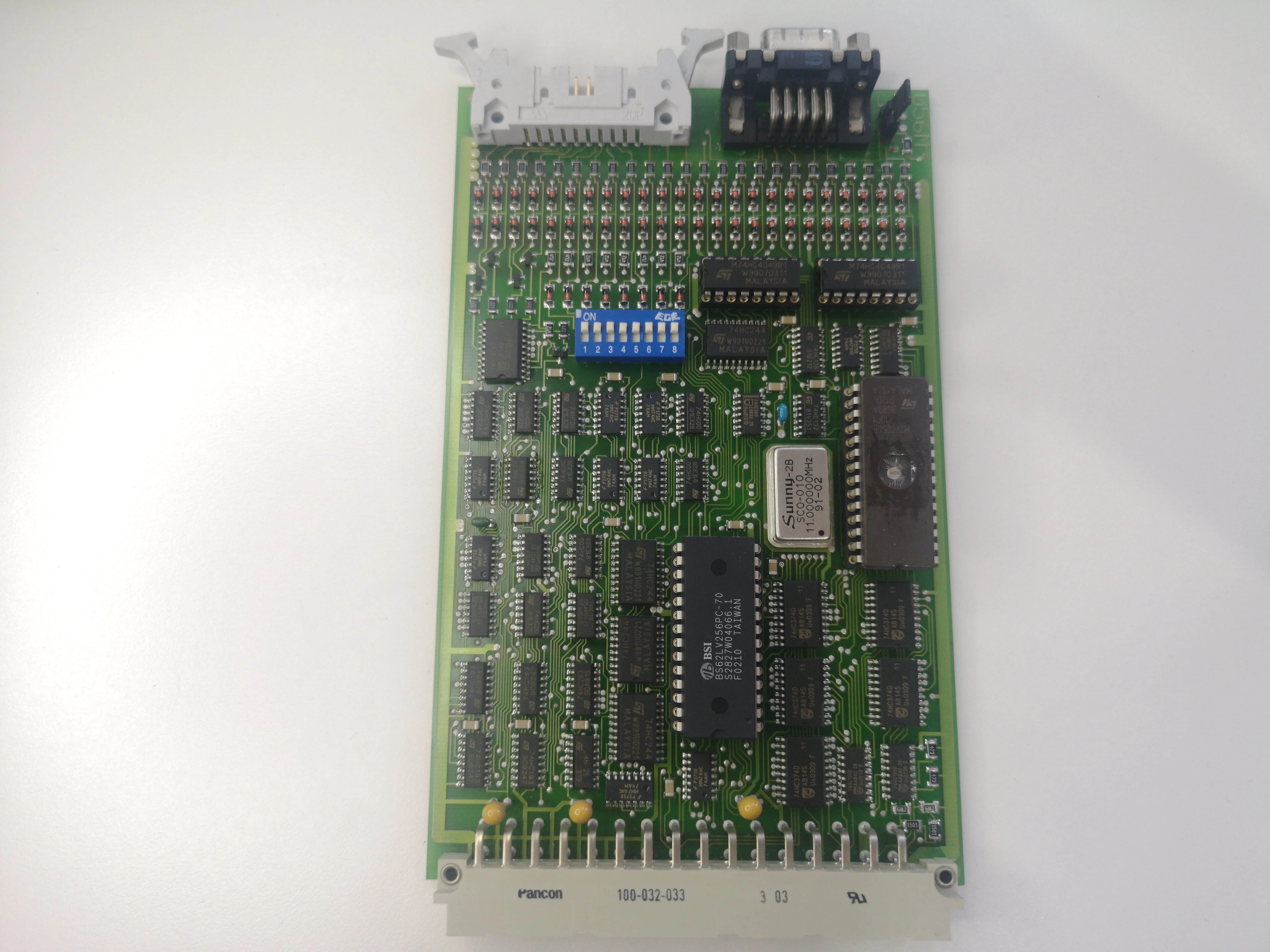
What immediately caught my eye was one of the boards, right after the processor board. It appeared to be some sort of graphics card, and unlike all the other boards, it used SMD chips as well as DIP. It also had its own SRAM, EEPROM and rows with tons of diodes. Asking my friend about it, I discovered that it was used to connect the monitor and the input devices, however since they didn’t work, the PLC had no way of communicating with the outside world. This made me realize that I had no real way of actually using this PLC, however before I fixed that I took a look at the other boards that comprised it.
The processor board
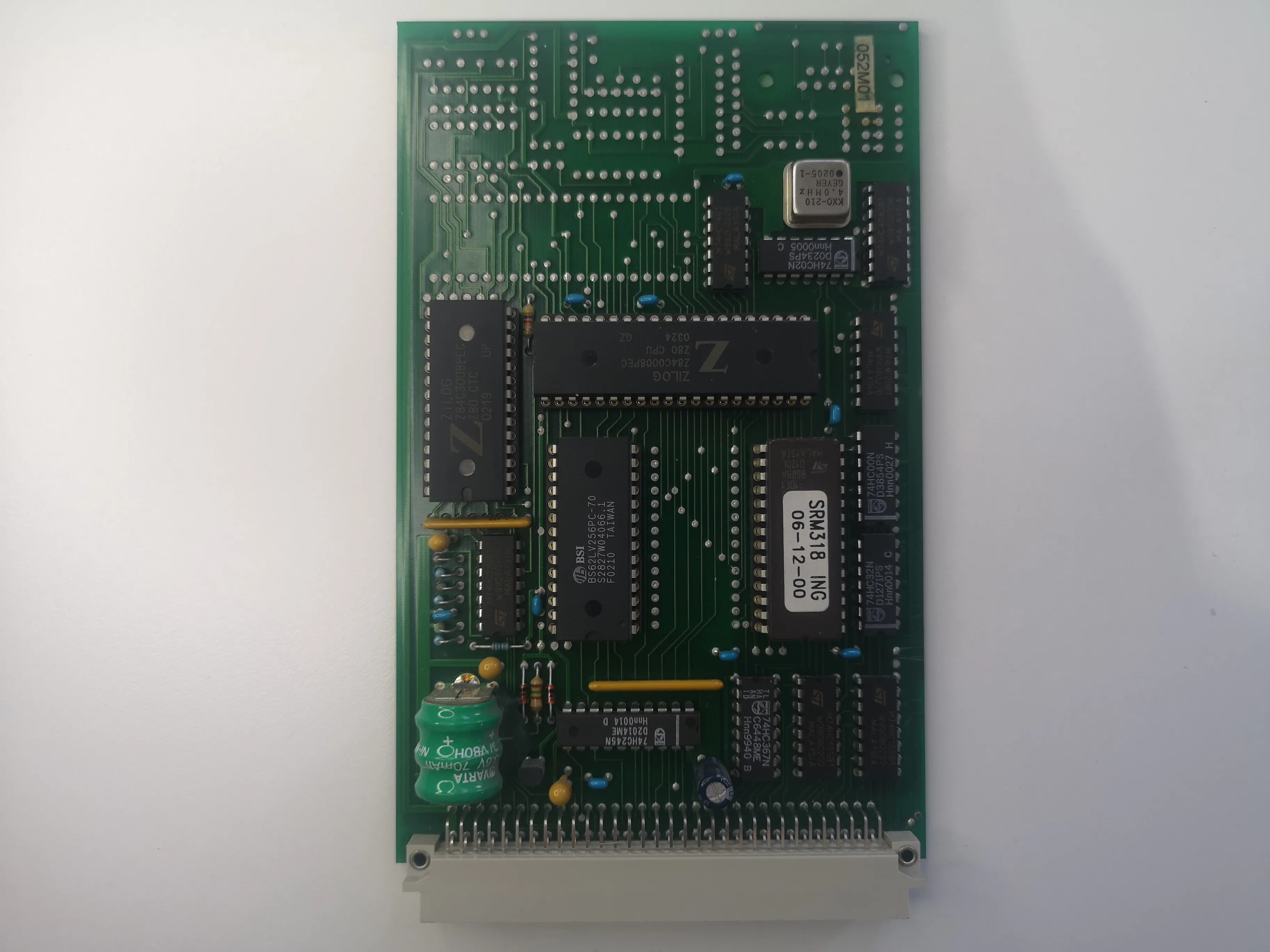
This board is the processor board, featuring the Z80, an EEPROM, an SRAM and the Z80 CTC (counter/timer chip). Interestingly, there is space on the board for many more chips, which most likely would have been Z80 SIO/PIO for parallel or serial communication, however I am not sure yet. The CPU runs at 4MHz, however the Z80 basically divides the clock by 4, meaning that the CPU is running at an effective speed of 1MHz. For modern standards, this is extremely slow, however it is likely that for an industrial process, this would be more than enough.
This PLC would likely have been used to control small motors and monitor processes, for which the speed is enough. The SRAM is only 32KB, and there appears to be space for another one, however that likely would have required more Z80 address decoding, and given the functionality of the PLC, I doubt the SRAM would have been required. Even 32KB is a lot in most embedded cases.
This board uses a 74HC245 bus transceiver coupled with a few 74HC155 line decoders, meaning that the rest of the boards are simply used as peripheral devices of the Z80. This is one of the reasons why such a discrete CPU design is a good fit for embedded purposes, since an almost infinite number of devices can be added to the bus by simply just adding more line decoders. However, I am unsure of why they went specifically with the Z80, as an 8051 or similar microcontroller with external data/code capability would have also been able to do the job, however it would have required many less chips for the same functionality.
Reading the EEPROMs revealed a lot of Z80 code, and interestingly strings for a user interface that could have been switched between both Italian and English. In many of the error messages, pumps, motors and glass-production-related phrases were mentioned, indicating that this was likely used in a field related to that, but I have no information at all about what this PLC was used for. There is no information about it online, and I did manage to contact the company, however they just responded with stating that they are unable to share details about it. Since I don’t plan on using the Z80 and the “graphics card”, I chose to focus on the other boards and see what I can get from the system.
The power board
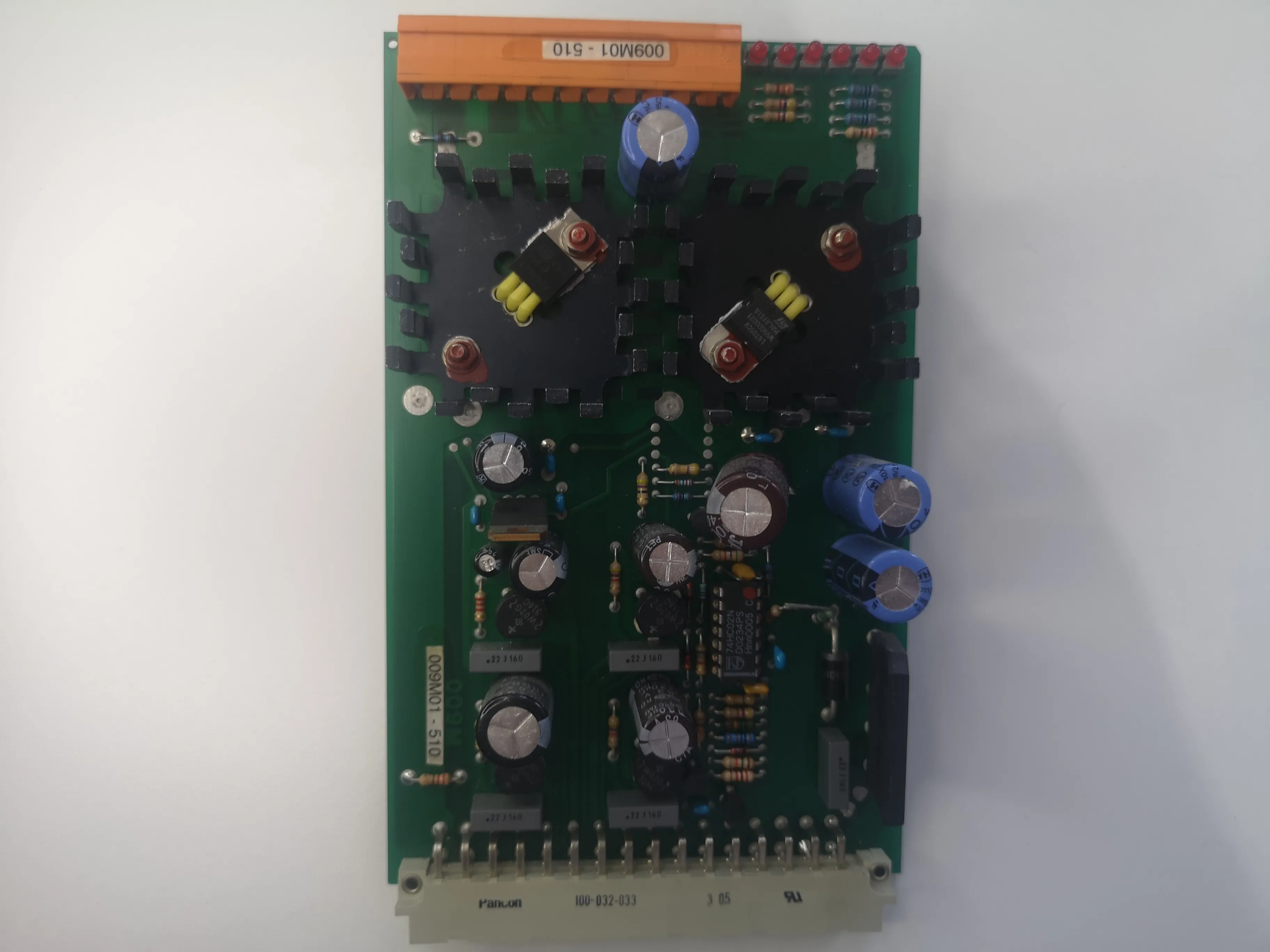
The power supply board initially appeared completely fine. It used three different linear regulators to obtain a 5V rail, which was strange, however it looked well-made, and I found it interesting that a 74HC32 (or-gate logic chip) was used for some purpose in a power supply. There are four main power rails coming from the large 75VA toroidal transformer: 5V, 12V, 15V and -15V, however only the 5V rail has power regulators on this board. How this is handled will be seen later, but for now while we’re still on this board it is interesting to note that two capacitors have been replaced, and given the specific brand and model of capacitor, I believe I know exactly where they were purchased.
However, the repair appears to have missed the fact that on the other side of the board, there is a massive electrolytic capacitor with heavy physical damage – it looked like a squished can. This obviously would severely degrade the capacitance, and I didn’t even attempt to power the board, given the danger a massive damaged electrolytic capacitor with no brand markings could be. Still, the board appears to be very well-made and the regulators are heatsinked, there are many zener diodes which monitor the voltage and the branded, non-replaced capacitors are all from reputable manufacturers. If I ever need to salvage good linear regulators with heatsinks, I will take this board apart, or even attempt to replace the large, damaged capacitor and make it work again. For now, though onto the next board.
The ADC board
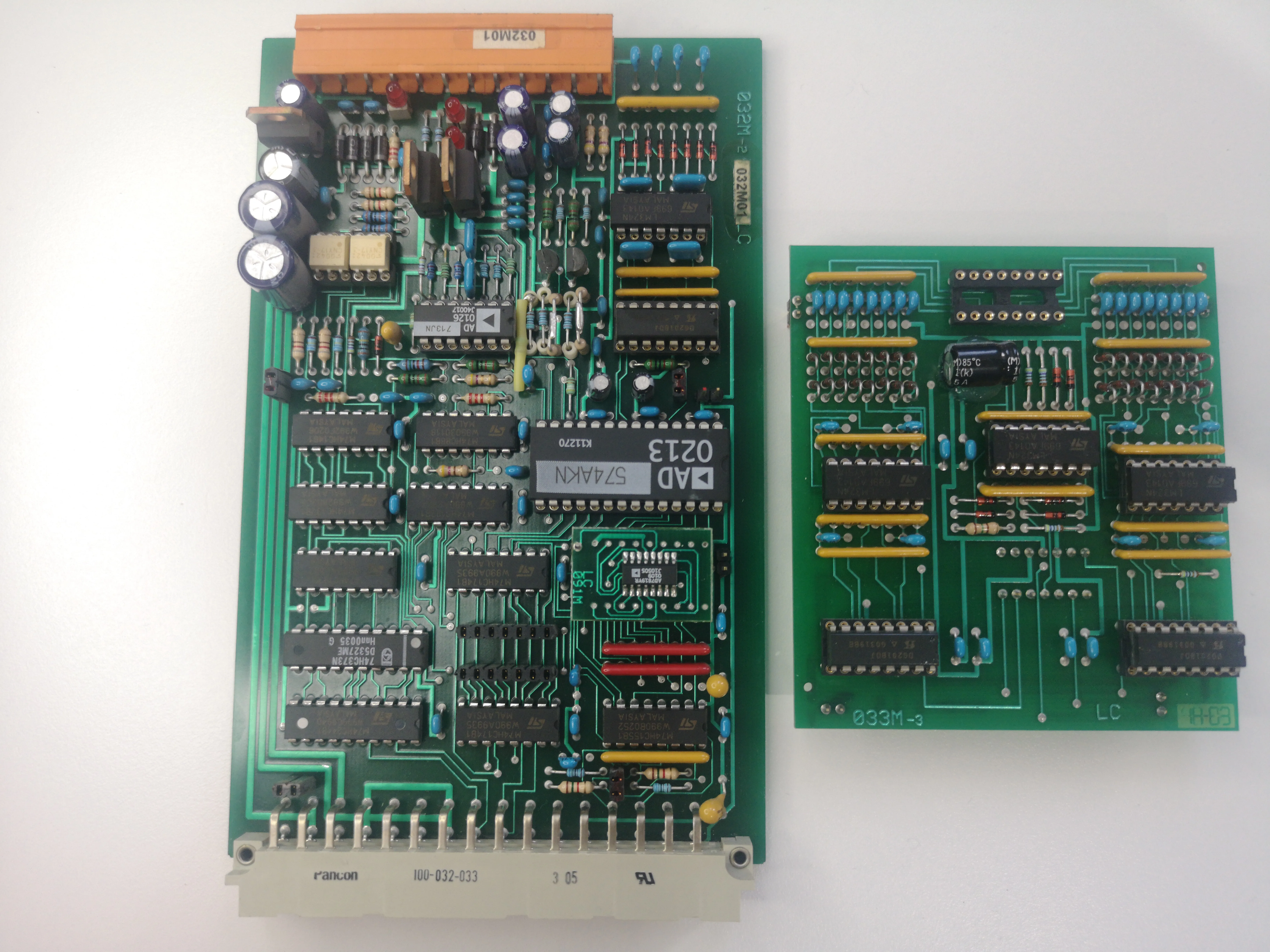
The ADC board is the most densely populated board (apart from the graphics, however that was SMD) in the whole system. The highlight of the board is the AD574AKN ADC, which is a high-quality 12-bit ADC, albeit a quite slow one with a 35 microsecond maximum conversion time, given that it uses successive approximation. With the ability to interface with 8-bit microprocessors, it is a perfect fit for such a system. If that isn’t fast enough, another ADC, the AD7819 is also present on a SMD-to-DIP adapter. This is an 8-bit ADC with a 4.5 microsecond conversion time, likely for when you want a less-accurate but faster result. The ADCs are fed with a ±15V regulated voltage, allowing for a significantly wide range.
The most interesting part about the board is the add-on board containing a massive number of diodes and resistor packs. I do not know what this board is used for, and the design for the ADC appears to have had the most issues during design, judging from the SMD-add-on 8-bit ADC and extra board. The ADC by modern standards is obsolete, as even a simple 32-bit ARM will contain a 12-bit ADC with comparable performance, while not having to take up large board space and special addressing. As such, this board for my purposes is quite useless, apart from the beautiful design.
The optocoupler board
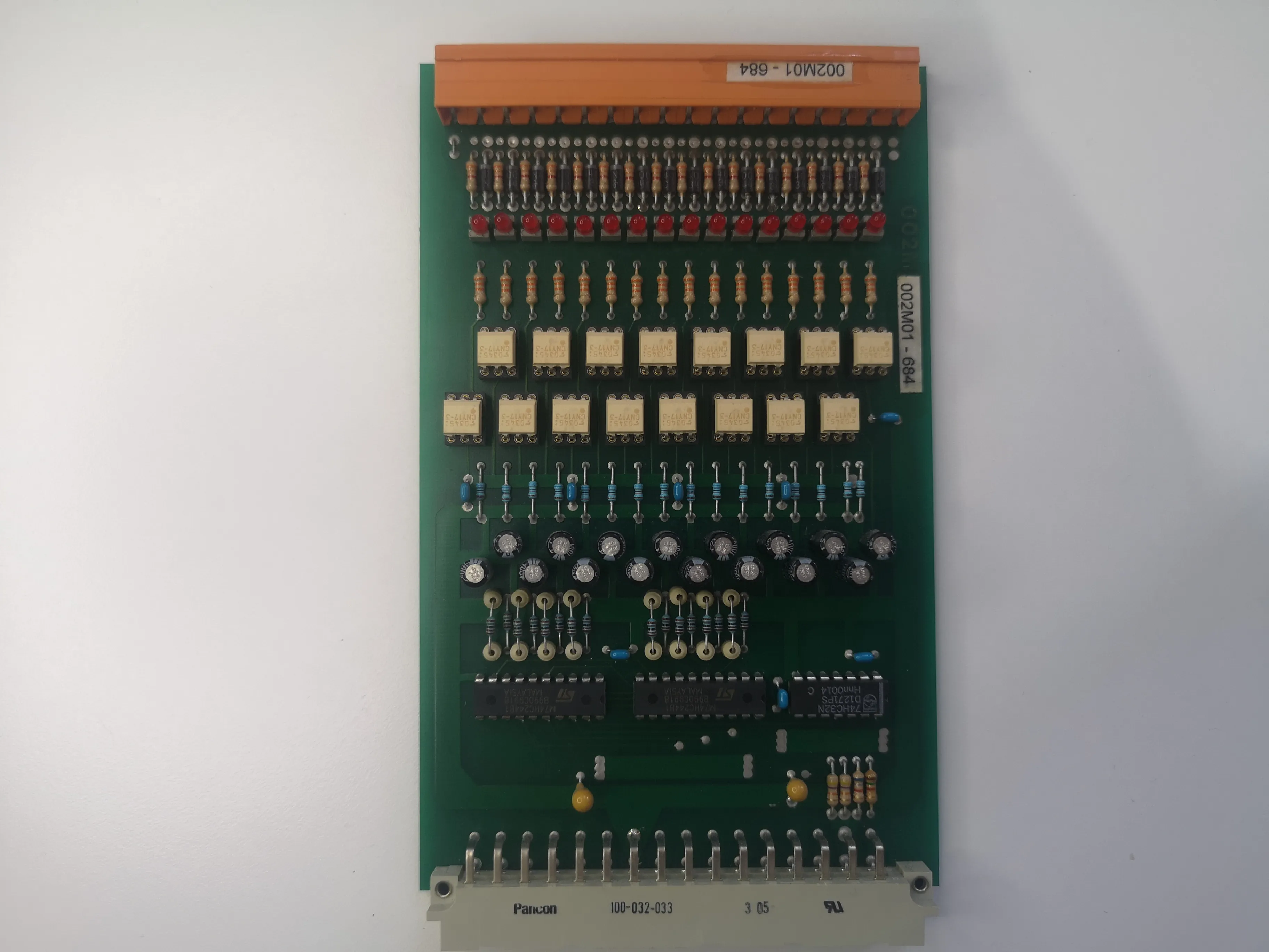
The PLC contains three separate boards with optocoupler inputs, with 16 inputs per board. The optocouplers used are quite cheap and simple, however the design of the boards really makes them shine. Featuring reverse voltage protection diodes, indicator LEDs, individual smoothing electrolytic capacitors for each channel and significant physical isolation, the design appears rock-solid. The optocouplers use simple 74HC244 bus transceivers controlled by the multiplexers to send data to the CPU.
Since these optocouplers are meant for a maximum of 110KHz operation, they can’t be used for any fast digital systems, however for industrial uses it is likely that they are fast enough for about anything. Again, the components in this PLC are limited mostly by the glacially slow (by modern standards) CPU. Finally, what I like most about this board is the mesmerizing patters created by so many identical and parallel components.
The relay board
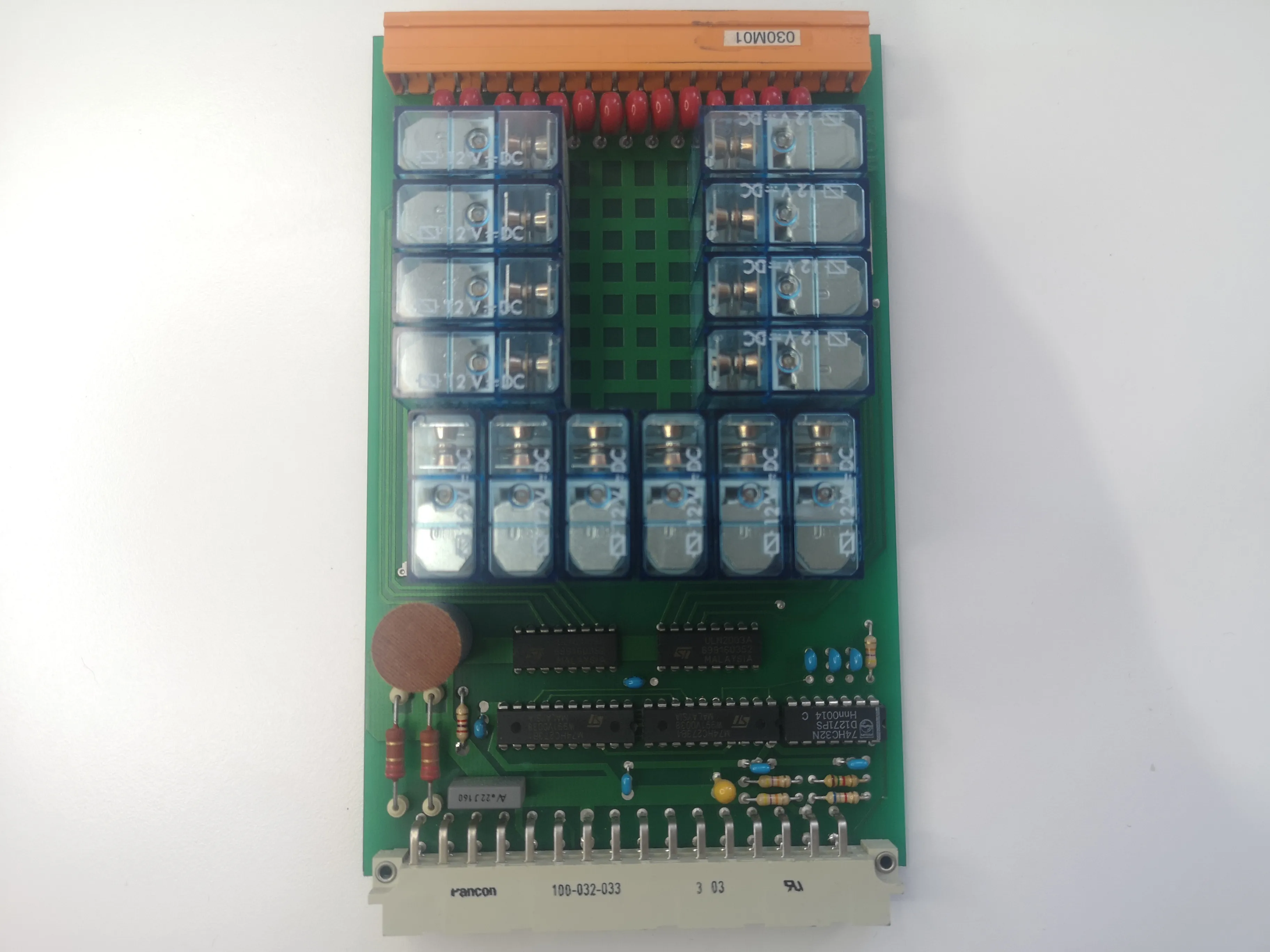
The final board type, and the one which I am repairing this PLC for, is the relay board. Containing 14 relays with a maximum of 10A250V operation, these relays can control a lot of different electrical equipment. Since I have a lack of relays, and wanted to learn more about them, figuring out how this board works and using it was a top priority with the PLC.
The overall architecture of the board is really simple - two 74HC273 latches have data sent to them by the CPU, and the latches then hold a value which is sent to two ULN2003 Darlington arrays, which turn the relays on. However, having no knowledge of the control signals of the board, I had to go through the difficult task of figuring out each control line and how it is connected to the CPU, so that I could set up a microcontroller to emulate it.
Initially I found out the 12V, 5V and GND lines by probing with my multimeter and visually tracing the lines, as they were thick. It is interesting to note that the 12V line is completely unregulated, only rectified and smoothed by capacitors, with low-value series resistors between the unregulated power and the relays. The 5V line, on the other hand, contains many filtering capacitors all throughout the PLC, likely since in a industrial environment with high voltages and currents switching everywhere, noise can become an issue.
After the power pins were marked, it was time to figure out how the Z80 controlled the latches. Firstly, I needed to find out how the 74HC32 is connected and decoding the signals. The latches have two important external signals - clock and clear. Clear is an active-low signal that sets all the outputs to zero, while clock is used to latch in the data. Since the Z80 only has an 8-bit data bus, two separate clock signals would be needed for each, and one signal would be needed for the clear output. Using a multimeter revealed that the signals were connected in an interesting way - two OR gates were used for clock signals, and the OR gates could either be controlled individually, or one signal to turn on both of them. The remaining two OR gates were used as buffers, with three separate capacitors to ground and a 1.5K pull-down resistor. It appears as if a lot of care was taken so that the default state of all relays would be for them to be turned off unless driven high by a decently powerful signal, such as a CMOS push-pull output pin.
After I traced out the control signals, I went to look at the data connections. Since the ULN2003 controls seven relays, and each is indeed connected to seven relays, one data pin from the 74HC273s would be redundant, as they are 8-bit latches. Interestingly, once all the signals were traced out, it turned out that the redundant bits were connected, likely to avoid using a pull-up/pull-down resistor, and the output was just left floating. Once I had all the inputs figured out, it was time to actually control the board. One thing I found unusual about the signals was how the input bits appeared to have no sequential relation, and relays appeared to be connected based on routing convenience, rather than sequential order.
The connectors on the edges of every board were of the DIN 41612 variety, and were even helpfully labelled with a manufacturer’s code. Once I found out they were ~15$ per connector, my handling of the board became more delicate, as I realized the kidney’s worth of premium connectors this PLC had. However, luckily for me, the pin pitch was a regular 5.08mm, or two DIP pins. This meant that I could use two rows of regular female DIP headers to make a decent connection with the board. After about two hours of soldering things on a perfboard, which included adding a 5V regulator from the 12V line and making a convenient header to connect external signals, I attached my DIY adapter to the board. I connected my semi-DIY power supply to the 12V headers, and then I looked for something to talk to it with. Initially, since I knew that the controlling of the relays could just involve one clock signal, I connected one of the 74HC273’s write pins and manually inserted it into ground and then 5V again, with another pin used to set relays manually. I did this to figure out how every relay was connected, so that I could complete the reverse engineering of the relay board. After one connection, I became bored, so I just wrote a quick Arduino script to do it for me, however since I was too bored to program each Arduino pin necessary, I just used it to drive the write and clear signals, while I manually connected each relay’s associated data pin to 5V and observed which one turned on. This method worked perfectly, and in less than five minutes I had figured out the direct pin connections to all relays.
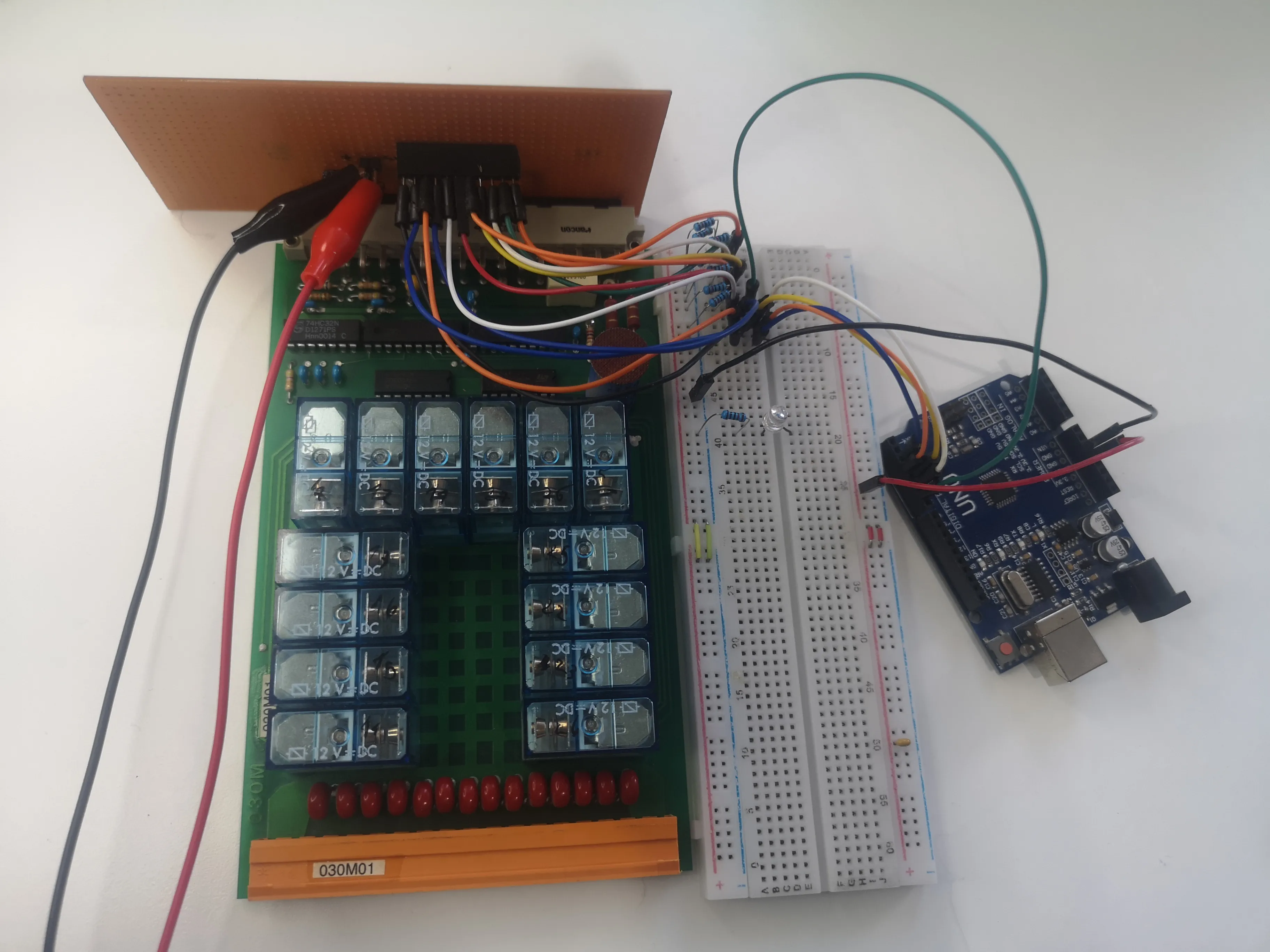
Finally, once the whole process was complete, I sat back and thought about what I could now do with 42 quality relays. The relays being 12V was an issue, as well as them consuming ~500mW per relay, which is very inconvenient. If all the relays were turned on, they would consume at least 7W, and if I used every board, I’d need a power supply with at least 21W, and that’s disregarding any losses and relays which consume more power than others. Accounting for tolerances, I’d need at least a beefy power supply, and my first thought went to a laptop power supply with a buck converter. Laptop power supplies provide cheap 19V rails, although quite noisy ones, which is absolutely not an issue with relays.
Furthermore, another improvement to make would be replacing the Z80 CPU board with something more modern, which can be talked to by modern equipment. Ideas for this were an ESP32 or a 32-bit ARM/RISC-V with an NRF24L01+, however anything more powerful than a Z80 would suffice, which would mean just about any microcontroller for sale at the moment. The idea of adding RISC-V to it sound most attractive, as I have three CH32V307F and one GD32VF103 RISC-V microcontrollers which are nice to work with, can be used with an RTOS like RT-Thread, and actually miraculously available to buy on places like LCSC. However, both of these ideas are to be left for another time, as it is now time to resume with another project - something with the 8051/8048 microcontrollers! As if I hadn’t spent the past 2400 words mocking the Z80…
